3.2.3. Design optimization parameters
Memory access interleaving
By default, FPGA memory is allocated sequentially.
By setting the --memory_interleaving_stride=<stride> option will result
in allocations being placed in different modules each stride bytes.
Therefore accelerator memory accesses will be scattered across the different memory interfaces.
For instance, setting --memory_interleaving_stride=4096.
Will result in the first 4k being allocated to bank 0,
next 4k are allocated info bank 1, and so on.
This may improve accelerator memory access bandwidth when combined with the Interconnect optimization strategy option:
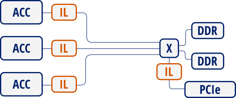
Memory interconnection with memory interleaving enabled
Interconnect optimization strategy
Option --interconnect_opt=<optimization strategy> defines the optimization strategy
for AXI interconnects.
This option only accepts area or performance strategies.
While area results in lower resource usage,
performance is lower than the performance setting.
In particular, using area prevents access from different slaves into different masters do be performed in parallel.
See also Xilinx PG059 for more details on the different strategies.
Interconnect register slices
By specifying --interconnect_regslices option,
it enables outer and auto register slice mode on interconnect cores.
This mode places an extra outer register between the inner interconnect logic (crossbar, width converter, etc.) and the outer core slave interfaces. It also places an auto register slice if the slave interface is in the same clock domain. See Xilinx PG059 for details on these modes.